|
|
请教有用过的samsung mcu 的大哥。
开发环境: iar for sam8
请教问题1 : 在iar for sam8里能否软件仿真中断?
2 : 如果可以,什么设置?
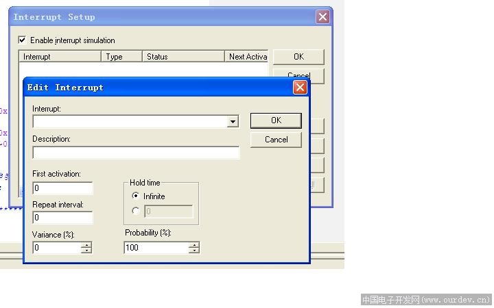
(原文件名:1.JPG)
3 : 我的代码如下,为什么烧写到目标板也不能中断?
//********************************
//使用MCU: S3F9488
//FOSC = 4.194MHZ
//********************************
#include "ioS3C9488.h"//
#include "iobit.h" //IO端口位操作定义文件
//************************************************
//**此处为宏定义替换******
#define uchar unsigned char
#define uint unsigned int
#define nop (__no_operation())
#define di (__disable_interrupt())
#define ei (__enable_interrupt())
//#define di() SYM&=0x07
//#define ei() SYM|=0x08
#define Clr_WatchDog() WDTCON = 0xfa
#define Buzzer_Enable() WTCON |=0x02
#define Buzzer_Disable() WTCON &=~0x02
__root __interrupt void int_9488();
//__code const volatile uchar SmartOption[4] @0x003c = {0x0,0x0,0x4c,0x05};
__root __code const volatile uchar SmartOption1 @0x003c = 0xFF;
__root __code const volatile uchar SmartOption2 @0x003d = 0xff;
__root __code const volatile uchar SmartOption3 @0x003e = 0x2F;
__root __code const volatile uchar SmartOption4 @0x003f = 0xFD;
//--------------------------------------------------------
//位操作
////Set_Bit(P0,0); //P00=1
//Clr_Bit(P0,0); //P00=0
//Com_Bit(P0,0); //P00=!P00
//if(Test_Bit(P0,0)) Set_Bit(P0,1) ; //如果P00=1,则P01=1
#define Set_Bit(byte,bit) (byte|=(1<<bit)) //置位
#define Clr_Bit(byte,bit) (byte&=~(1<<bit)) //清零
#define Com_Bit(byte,bit) (byte^=(1<<bit)) //取反
#define Test_Bit(byte,bit) (byte&(1<<bit)) //测试
//--------------------------------------------------------
//****启动时IO初始化子过程******
void chip_init()
{
SYM = 0X00;
OSCCON=0x00; //main osc run,sub osc stop,select main osc
// OSCCON=0x04; //main osc run,sub osc run,select main osc
//CLKCON— System Clock Control Register D4H
//7 Oscillator IRQ Wake-up Function Enable Bit
//0 Enable IRQ for main system oscillator wake-up function
//1 Disable IRQ for main system oscillator wake-up function
//6-5 Not used for the S3C9484/C9488/F9488
//4-3 CPU Clock (System Clock) Selection Bits (note)
//0 0 fxx/16
//0 1 fxx/8
//1 0 fxx/2
//1 1 fxx/1 (non-divided)
//2-0 Not used for the S3C9484/C9488/F9488
CLKCON = 0x98; //Enable IRQ,Fosc/1
P0CONH = 0x95;
P0CONL = 0x02;
P0 = 0x80;
P0PUR = 0x89;
P1CONH = 0xaa;
P1CONL = 0xa9;
P1 = 0xff;
P1PUR = 0xff;
P2CONH = 0x02;
P2CONL = 0xaa;
P2 = 0xff;
P3CONH = 0xff;
P3CONL = 0x00;
P3INT = 0x23;
P3 = 0x00;
P3PND=0x00;
P4CONH = 0xa;
P4CONL = 0xaa;
P4 = 0x00;
//WTCON— Watch Timer Control Register F9H
//7 Watch Timer Clock Selection Bit
//0 Main system clock divided by 27 (fxx/128)
//1 Sub system clock (fxt)
//6 Watch Timer Interrupt Enable Bit
//0 Disable watch timer interrupt
//1 Enable watch timer interrupt
//5–4 Buzzer Signal Selection Bits
//0 0 0.5 kHz buzzer (BUZ) signal output
//0 1 1 kHz buzzer (BUZ) signal output
//1 0 2 kHz buzzer (BUZ) signal output
//1 1 4 kHz buzzer (BUZ) signal output
//3–2 Watch Timer Speed Selection Bits
//0 0 1.0 s Interval
//0 1 0.5 s Interval
//1 0 0.25 s Interval
//1 1 3.91 ms Interval
//1 Watch Timer Enable Bit
//0 Disable watch timer; Clear frequency dividing circuits
//1 Enable watch timer
//0 Watch Timer Interrupt Pending Bit
//0 Interrupt is not pending, Clear pending bit when write
//1 Interrupt is pending
WTCON = 0x76; //main osc/128,0.5的中断作为实时时钟的时钟源,4Khz Buzzer
STPCON = 0X00; //disable stop instruction
//BTCON — Basic Timer Control Register DCH
//7-4 Not used for the S3C9484/C9488/F9488
//3-2 Basic Timer Input Clock Selection Bits
//0 0 fxx/4096 (3)
//0 1 fxx/1024
//1 0 fxx/128
//1 1 Not used
//1 Basic Timer Counter Clear Bit (1)
//0 No effect
//1 Clear the basic timer counter value
//0 Clock Frequency Divider Clear Bit for Basic Timer (2)
//0 No effect
//1 Clear both clock frequency dividers
// BTCON = 0X00; //
//TACON— Timer A Control Register F3H
//7-6 Timer A Input Clock Selection Bits
//0 0 fxx/1024
//0 1 fxx/256
//1 0 fxx/64
//1 1 External clock (TACK)
//5-4 Timer A Operating Mode Selection Bits
//0 0 Internal mode (TAOUT mode)
//0 1 Capture mode (capture on rising edge, counter running, OVF can occur)
//1 0 Capture mode (capture on falling edge, counter running, OVF can occur)
//1 1 PWM mode (OVF interrupt can occur)
//3 Timer A Counter Clear Bit
//0 No effect
//1 Clear the timer A counter (After clearing, return to zero)
//2 Timer A Overflow Interrupt Enable Bit
//0 Disable interrupt
//1 Enable interrupt
//1 Timer A Match/Capture Interrupt Enable Bit
//0 Disable interrupt
//1 Enable interrupt
//0 Timer A Start/Stop Bit
//0 Stop Timer A
//1 Start Timer A
//时钟初始化,计数模式,开始计数
//TACON = 0x8d; //clock=fxx/1024,enable interrupt
TACON = 0X4B; //TA FXX/1024,internal mode,clear time a,enable ta,start time a
TADATA = 100; //TIME=1/(4.19M/1024)*n=10ms
//TBCON— Timer B Control Register F8H
//7-6 Timer B Input Clock Selection Bits
//0 0 fxx
//0 1 fxx/2
//1 0 fxx/4
//1 1 fxx/8
//5–4 Timer B Interrupt Time Selection Bits
//0 0 Elapsed time for low data value
//0 1 Elapsed time for high data value
//1 0 Elapsed time for low and high data values
//1 1 Invalid setting
//3 Timer B Underflow Interrupt Enable Bit
//0 Disable Interrupt
//1 Enable Interrupt
//2 Timer B Start/Stop Bit
//0 Stop timer B
//1 Start timer B
//1 Timer B Mode Selection Bit
//0 One-shot mode
//1 Repeating mode
//0 Timer B Output flip-flop Control Bit
//0 T-FF is low
//1 T-FF is high
//时钟8分频,工作模式11,连续模式
TBDATAL = 0X2; //10ms,
TBDATAH = 0X2; //高低字节型,低字节没有用到
TBCON = 0xDE; //fxx/8
//LCDCON — LCD Control Register D0H
//7 LCD Module enable/disable Bit
//0 Disable LCD Module
//1 Enable LCD Module
//6 Not used for the S3C9484/C9488/F9488
//5-4 LCD Duty Selection Bit
//0 0 1/8 duty , 1/4 bias
//0 1 1/4 duty , 1/3 bias
//1 x Static
//3-2 LCD Dot On/Off Control Bits
//0 0 Off signal
//0 1 On signal
//1 x Normal display
//1-0 LCD Clock Signal Selection Bits
//0 0 fw/27
//0 1 fw/26
//1 0 fw/25
//1 1 fw/24
LCDCON=0x00; //Disable LCD module
//TINTPND — Timer A,B Interrupt Pending Register F2H
//7-3 Not used for the S3C9484/C9488/F9488
//2 Timer B Underflow Interrupt Pending Bit
//0 No interrupt pending
//0 Clear pending bit when write
//1 Interrupt pending
//1 Timer A Overflow Interrupt Pending Bit
//0 No interrupt pending
//0 Clear pending bit when write
//1 Interrupt pending
//0 Timer A Match/Capture Interrupt Pending Bit
//0 No interrupt pending
//0 Clear pending bit when write
//1 Interrupt pending
//中断标志位
// TINTPND=0x00;
//UARTCON— UART Control Register FDH
//7-6 Operating mode and baud rate selection bits
//0 0 Mode 0: Shift Register [fxx/(16 ′ (16bit BRDATA + 1))]
//0 1 Mode 1: 8-bit UART [fxx/(16 ′ (16bit BRDATA + 1))]
//1 x Mode 2: 9-bit UART [fxx/(16 ′ (16bit BRDATA + 1))]
//5 Multiprocessor communication(1) enable bit (for modes 2 only)
//0 Disable
//1 Enable
//4 Serial data receive enable bit
//0 Disable
//1 Enable
//3 If Parity disable mode (PEN = 0),
//Location of the 9th data bit to be transmitted in UART mode 2 ("0" or "1").
//If Parity enable mode (PEN = 1),
//even/odd parity selection bit for transmit data in UART mode 2.
//0: Even parity bit generation for transmit data
//1: Odd parity bit generation for transmit data
//2 If Parity disable (PEN = 0),
//location of the 9th data bit that was received in UART mode 2 ("0" or "1").
//If Parity enable mode (PEN = 1),
//even/odd parity selection bit for receive data in UART mode 2.
//0: Even parity check for the received data
//1: Odd parity check for the received data
//A result of parity error will be saved in RPE bit of the UARTPND register after parity
//checking of the received data.
//1 Receive interrupt enable bit
//0 Disable Receive interrupt
//1 Enable Receive interrupt
//0 Transmit interrupt enable bit
//0 Disable Transmit interrupt
//1 Enable Transmit Interrupt
//
UARTCON=0x00;
//UARTPND— UART Pending and parity control FEH
//7-6 Not used for the S3C9484/C9488/F9488
//5 UART parity enable/disable (PEN)
//0 Disable
//1 Enable
//4 UART receive parity error (RPE)
//0 No error
//1 Parity error
//3-2 Not used for the S3C9484/C9488/F9488
//1 UART receive interrupt pending flag
//0 Not pending
//0 Clear pending bit (when write)
//1 Interrupt pending
//0 UART transmit interrupt pending flag
//0 Not pending
//0 Clear pending bit (when write)
//1 Interrupt pending
UARTPND=0x00;
//VLDCON— Voltage Level Detector Control Register D8H
//7 Not used for the S3C9484/C9488/F9488
//6 VLD Level Set Bit
//0 VDD is higher than reference voltage
//1 VDD is lower than reference voltage
//5-1 Reference Voltage Selection Bits
//10110 VVLD = 2.4 V
//10011 VVLD = 2.7 V
//01110 VVLD = 3.3 V
//01011 VVLD = 3.9 V
//Other values Don’t care
//0 VLD Operation Enable Bit
//0 Operation off
//1 Operation on
// VLDCON = 0x67; //2.7V
ADCON = 0x57;
return;
}
void delay(void)
{
unsigned char i,j;
for(i=200;i>0;i--)
for(j=200;j>0;j--);
}
unsigned char Temp=0;
int main()
{
chip_init();
// Clr_WatchDog();
SYM|=0X08;
while(1)
{
Temp++;
// Clr_WatchDog();
// Com_P00;
// PortBuzzer_Inverse(); //P1.1 取反
}
}
//**中断向量及服务程序定义********
#pragma vector = __TIMERA_OVERFLOW_vector
__interrupt void int_9488()
{
PortBuzzer_Inverse(); //P1.1 取反
Com_P00;
if(TINTPND&0x01) //TA capture/match
{
TINTPND&=~0x01;
}
if(TINTPND&0x02) //TA OVERFLOW
{
TINTPND&=~0x02;
}
if(TINTPND&0x03) //TB OVERFLOW
{
TINTPND&=~0x03;
}
if(P3PND&0x01) //P3.3
{
P3PND&=~0x01;
}
if(P3PND&0x02) //P3.4
{
P3PND&=~0x02;
}
if(P3PND&0x04) //P3.5
{
P3PND&=~0x04;
}
if(P3PND&0x08) //P3.6
{
P3PND&=~0x08;
}
} |
阿莫论坛20周年了!感谢大家的支持与爱护!!
曾经有一段真挚的爱情摆在我的面前,我没有珍惜,现在想起来,还好我没有珍惜……
|


 发表于 2011-11-9 23:21:04
 楼主
楼主