|
|
 发表于 2013-3-31 09:01:14
|
显示全部楼层
发表于 2013-3-31 09:01:14
|
显示全部楼层
myjnj 发表于 2011-11-12 22:45 
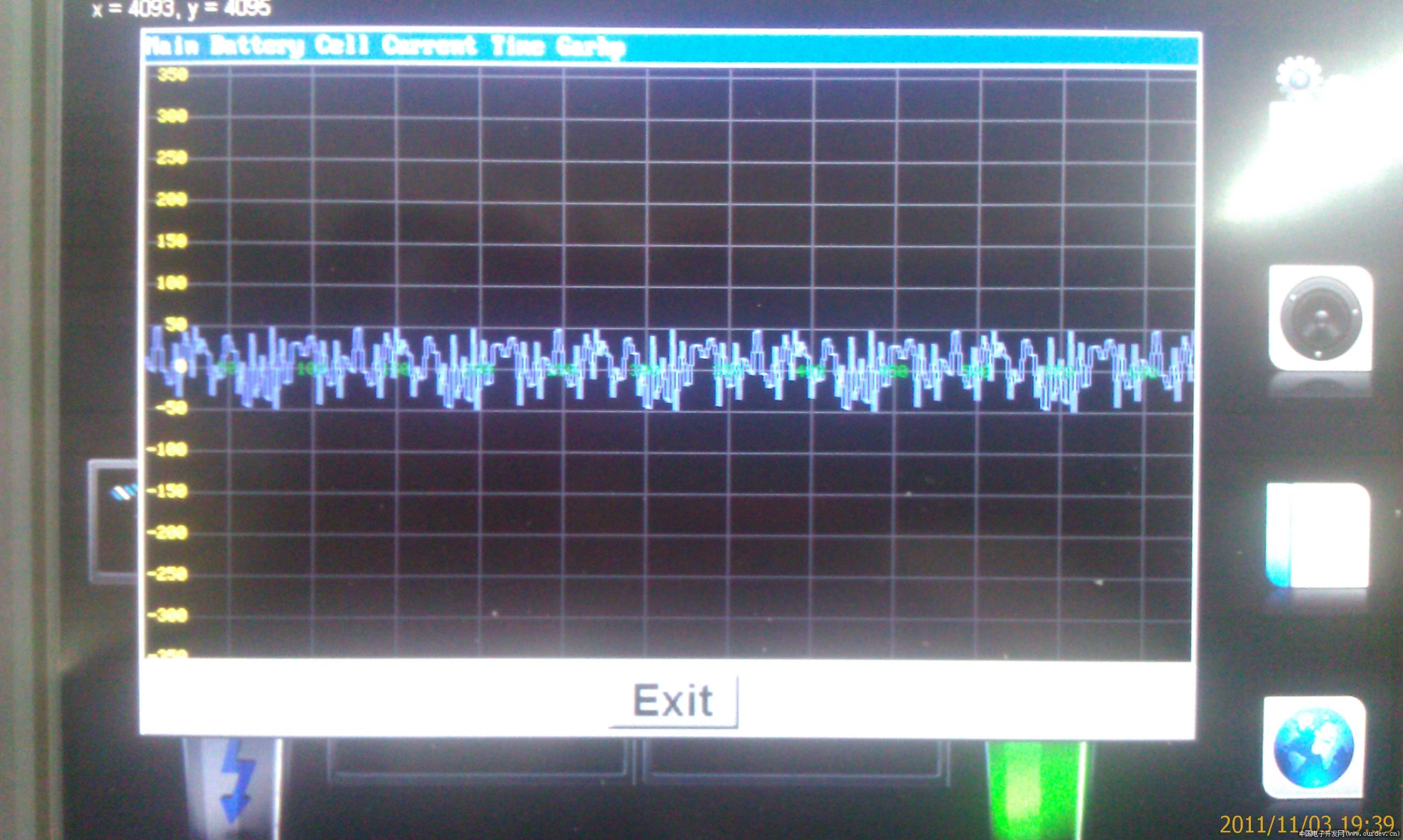
我发现驱动640x480的TFT, 静态显示很好,在写屏或者向SDRAM中写的时候, 显示会明显的闪烁/花屏
硬件设置 ...
请问一下你这个问题解决了吗?
我最近也在用1788的板子,屏幕480*800
也是好像在操作sdram的时候有问题。
这个板子的测试程序:
#define SYS_FREQ 60MHZ
//#define SYS_FREQ 108MHZ
#if SYS_FREQ == (120MHZ)
#define SDRAM_PERIOD 8.33 // 120MHz
#elif SYS_FREQ == (108MHZ)
#define SDRAM_PERIOD 9.25 // 108MHz
#elif SYS_FREQ == (96MHZ)
#define SDRAM_PERIOD 10.4 // 96MHz
#elif SYS_FREQ == (72MHZ)
#define SDRAM_PERIOD 13.8 // 72MHz
#elif SYS_FREQ == (60MHZ)
#define SDRAM_PERIOD 16.67 // 72MHz
#elif SYS_FREQ == (57MHZ)
#define SDRAM_PERIOD 17.4 // 57.6MHz
#elif SYS_FREQ == (48MHZ)
#define SDRAM_PERIOD 20.8 // 48MHz
#elif SYS_FREQ == (36MHZ)
#define SDRAM_PERIOD 27.8 // 36MHz
#elif SYS_FREQ == (24MHZ)
#define SDRAM_PERIOD 41.7 // 24MHz
#elif SYS_FREQ == (12MHZ)
#define SDRAM_PERIOD 83.3 // 12MHz
#else
#error Frequency not defined
#endif
#define P2C(Period) (((Period<SDRAM_PERIOD)?0:(uint32_t)((float)Period/SDRAM_PERIOD))+1)
#define SDRAM_REFRESH 7813
#define SDRAM_TRP 20
#define SDRAM_TRAS 45
#define SDRAM_TAPR 1
#define SDRAM_TDAL 3
#define SDRAM_TWR 3
#define SDRAM_TRC 65
#define SDRAM_TRFC 66
#define SDRAM_TXSR 67
#define SDRAM_TRRD 15
#define SDRAM_TMRD 3
volatile uint32_t i;
volatile unsigned long Dummy;
/************** init SDRAM **********/
/* init EMC_CAS */
LPC_IOCON->P2_16 = 0x21;
/* init EMC_RAS */
LPC_IOCON->P2_17 = 0x21;
/* init EMC_CLK0 */
LPC_IOCON->P2_18 = 0x21;
/* init EMC_DYCS0 */
LPC_IOCON->P2_20 = 0x21;
/* init EMC_CKE0 */
LPC_IOCON->P2_24 = 0x21;
/* init EMC_DQM0 */
LPC_IOCON->P2_28 = 0x21;
/* init EMC_DQM1 */
LPC_IOCON->P2_29 = 0x21;
/************** init SDRAM DATA PIN**********/
/* init EMC_D0 */
LPC_IOCON->P3_0 = 0x21;
/* init EMC_D1 */
LPC_IOCON->P3_1 = 0x21;
/* init EMC_D2 */
LPC_IOCON->P3_2 = 0x21;
/* init EMC_D3 */
LPC_IOCON->P3_3 = 0x21;
/* init EMC_D4 */
LPC_IOCON->P3_4 = 0x21;
/* init EMC_D5 */
LPC_IOCON->P3_5 = 0x21;
/* init EMC_D6 */
LPC_IOCON->P3_6 = 0x21;
/* init EMC_D7 */
LPC_IOCON->P3_7 = 0x21;
/* init EMC_D8 */
LPC_IOCON->P3_8 = 0x21;
/* init EMC_D9 */
LPC_IOCON->P3_9 = 0x21;
/* init EMC_D10 */
LPC_IOCON->P3_10 = 0x21;
/* init EMC_D11 */
LPC_IOCON->P3_11 = 0x21;
/* init EMC_D12 */
LPC_IOCON->P3_12 = 0x21;
/* init EMC_D13 */
LPC_IOCON->P3_13 = 0x21;
/* init EMC_D14 */
LPC_IOCON->P3_14 = 0x21;
/* init EMC_D15 */
LPC_IOCON->P3_15 = 0x21;
/************** init SDRAM ADDR PIN**********/
/* init EMC_A0 */
LPC_IOCON->P4_0 = 0x21;
/* init EMC_A1 */
LPC_IOCON->P4_1 = 0x21;
/* init EMC_A2 */
LPC_IOCON->P4_2 = 0x21;
/* init EMC_A3 */
LPC_IOCON->P4_3 = 0x21;
/* init EMC_A4 */
LPC_IOCON->P4_4 = 0x21;
/* init EMC_A5 */
LPC_IOCON->P4_5 = 0x21;
/* init EMC_A6 */
LPC_IOCON->P4_6 = 0x21;
/* init EMC_A7 */
LPC_IOCON->P4_7 = 0x21;
/* init EMC_A8 */
LPC_IOCON->P4_8 = 0x21;
/* init EMC_A9 */
LPC_IOCON->P4_9 = 0x21;
/* init EMC_A10 */
LPC_IOCON->P4_10 = 0x21;
/* init EMC_A11 */
LPC_IOCON->P4_11 = 0x21;
/* init EMC_A12 */
LPC_IOCON->P4_12 = 0x21;
/* init EMC_A13 */
LPC_IOCON->P4_13 = 0x21;
/* init EMC_A14 */
LPC_IOCON->P4_14 = 0x21;
/************** init SDRAM WE PIN**********/
/* init EMC_WE */
LPC_IOCON->P4_25 = 0x21;
/*
************************************
init SDRAM CONTROLLER
************************************
*/
/* Enable the EMC POWER */
LPC_SC->PCONP |= 0x00000800;
/*
Delay Control register (EMCDLYCTL - 0x400F C1DC)
The EMCDLYCTL register controls on-chip programmable delays that can b used to fine
tune timing to external SDRAM memories. Dela ys can be configured in increments of
approximately 250 picoseconds up to a maximum of roughly 7.75 ns.
*/
/*
Programmable delay value for EMC outputs in command delayed mode
The delay amount is roughly (CMDDLY+1) * 250 picoseconds
*/
LPC_SC->EMCDLYCTL |= (8<<0);
/*
Programmable delay value for the feedback clock that controls input data sampling
The delay amount is roughly (FBCLKDLY+1) * 250 picoseconds
*/
LPC_SC->EMCDLYCTL |=(8<<8);
/*
Programmable delay value for the CLKOUT0 output. This would typically be used in clock
delayed mode. The delay amount is roughly (CLKOUT0DLY+1) * 250 picoseconds.
*/
LPC_SC->EMCDLYCTL |= (0x08 <<16);
/*
Confige the EMC Register
*/
/*
EMC Control register (EMCControl - 0x2009 C000)
EMC Enable (E) = 1;
Address mirror (M) = 0; Normal memory map.
Low-power mode (L) = 0; Normal mode (warm reset value).
*/
LPC_EMC->Control =1;
/*
Dynamic Memory Read Configuration register (EMCDynamicReadConfig - 0x2009 C028)
1:0 Read data strategy (RD)
00 Clock out delayed strategy, using CLKOUT (command not delayed, clock out
delayed). POR reset value.
01 Command delayed strategy, using EMCCLKDELAY (command delayed, clock out
not delayed).
10 Command delayed strategy plus one clock cycle, using EMCCLKDELAY
(command delayed, clock out not delayed).
11 Command delayed strategy plus two clock cycles, using EMCCLKDELAY
(command delayed, clock out not delayed)
*/
LPC_EMC->DynamicReadConfig = 1;
/*
Dynamic Memory RAS & CAS Delay registers
The EMCDynamicRasCas0-3 registers enable you to program the RAS and CAS
latencies for the relevant dynamic memory
1:0 RAS latency (active to read/write delay) (RAS)
00 Reserved. 11
01 One CCLK cycle.
10 Two CCLK cycles.
11 Three CCLK cycles (POR reset value).
9:8 CAS latency (CAS)
00 Reserved. 11
01 One CCLK cycle.
10 Two CCLK cycles.
11 Three CCLK cycles (POR reset value).
*/
LPC_EMC->DynamicRasCas0 = 0;
LPC_EMC->DynamicRasCas0 |= (3<<8);
LPC_EMC->DynamicRasCas0 |= (2<<0);
/*
Dynamic Memory RAS & CAS Delay registers
The EMCDynamicRasCas0-3 registers enable you to program the RAS and CAS
latencies for the relevant dynamic memory
1:0 RAS latency (active to read/write delay) (RAS)
00 Reserved. 11
01 One CCLK cycle.
10 Two CCLK cycles.
11 Three CCLK cycles (POR reset value).
9:8 CAS latency (CAS)
00 Reserved. 11
01 One CCLK cycle.
10 Two CCLK cycles.
11 Three CCLK cycles (POR reset value).
*/
LPC_EMC->DynamicRasCas0 = 0;
LPC_EMC->DynamicRasCas0 |= (3<<8);
LPC_EMC->DynamicRasCas0 |= (3<<0);
/*
Dynamic Memory Precharge Command Period registe (EMCDynamictRP - 0x2009 C030)
The EMCDynamicTRP register enables you to program the precharge command period,
tRP.
3:0 Precharge command period (tRP)
0x0 - 0xE n + 1 clock cycles. The delay is in EMCCLK cycles.
0xF 16 clock cycles (POR reset value).
*/
LPC_EMC->DynamicRP = P2C(SDRAM_TRP);
/*
Dynamic Memory Active to Precharge Command Period register(EMCDynamictRAS - 0x2009 C034)
The EMCDynamicTRAS register enables you to program the active to precharge command period, tRAS.
3:0 Precharge command period (tRAS)
0x0 - 0xE n + 1 clock cycles. The delay is in EMCCLK cycles.
0xF 16 clock cycles (POR reset value).
*/
LPC_EMC->DynamicRAS = P2C(SDRAM_TRAS);
/*
Dynamic Memory Se lf-refresh Exit Time register(EMCDynamictSREX - 0x2009 C038)
The EMCDynamicTSREX register enables you to program the self-refresh exit time
3:0 Self-refresh exit time (tSREX)
0x0 - 0xE n + 1 clock cycles. The delay is in CCLK cycles.
0xF 16 clock cycles (POR reset value).
*/
LPC_EMC->DynamicSREX = P2C(SDRAM_TXSR);
/*
Dynamic Memory Last Data Out to Active Time register (EMCDynamictAPR - 0x2009 C03C)
The EMCDynamicTAPR register enables you to program the last-data-out to active
command time, tAPR.
3:0 Last-data-out to active command time (tAPR)
0x0 - 0xE n + 1 clock cycles. The delay is in CCLK cycles.
0xF 16 clock cycles (POR reset value).
*/
LPC_EMC->DynamicAPR = SDRAM_TAPR;
/*
Dynamic Memory Data-in to Active Command Time register (EMCDynamictDAL - 0x2009 C040)
The EMCDynamicTDAL register enables you to program the data-in to active command time, tDAL
3:0 Data-in to active command (tDAL)
0x0 - 0xE n + 1 clock cycles. The delay is in CCLK cycles.
0xF 16 clock cycles (POR reset value).
*/
LPC_EMC->DynamicDAL = SDRAM_TDAL + P2C(SDRAM_TRP);
/*
Dynamic Memory Wr ite Recovery Time regist er (EMCDynamictWR - 0x2009 C044)
The EMCDynamicTWR register enables you to pr ogram the write recovery time, tWR.
3:0 Write recovery time (tWR)
0x0 - 0xE n + 1 clock cycles. The delay is in CCLK cycles.
0xF 16 clock cycles (POR reset value).
*/
LPC_EMC->DynamicWR = SDRAM_TWR;
/*
Dynamic Memory Active to Active Command Period register (EMCDynamictRC - 0x2009 C048)
The EMCDynamicTRC register enables you to program the active to active command period, tRC.
3:0 Active to active command period (tRC)
0x0 - 0x1E n + 1 clock cycles. The delay is in CCLK cycles.
0xF 32 clock cycles (POR reset value).
*/
LPC_EMC->DynamicRC = P2C(SDRAM_TRC);
/*
Dynamic Memory Auto-refresh Period register (EMCDynamictRFC - 0x2009 C04C)
The EMCDynamicTRFC register enables you to program the auto-refresh period,
and auto-refresh to active command period, tRFC.
4:0 Auto-refresh period and auto-refresh to active command period (tRFC)
0x0 - 0x1E n + 1 clock cycles. The delay is in CCLK cycles.
0xF 32 clock cycles (POR reset value).
*/
LPC_EMC->DynamicRFC = P2C(SDRAM_TRFC);
/*
Dynamic Memory Exit Self-ref resh register (EMCDynamictXSR - 0x2009 C050)
The EMCDynamicTXSR register enables you to program the exit self-refresh to active
command time, tXSR.
4:0 Exit self-refresh to active command time (tXSR)
0x0 - 0x1E n + 1 clock cycles. The delay is in CCLK cycles.
0xF 32 clock cycles (POR reset value).
*/
LPC_EMC->DynamicXSR = P2C(SDRAM_TXSR);
/*
Dynamic Memory Active Bank A to Active Ba nk B Time register(EMCDynamictR RD - 0x2009 C054)
The EMCDynamicTRRD register enables you to program the active bank A to active bank B latency, tRRD.
3:0 Active bank A to active bank B latency (tRRD)
0x0 - 0x1E n + 1 clock cycles. The delay is in CCLK cycles.
0xF 16 clock cycles (POR reset value).
*/
LPC_EMC->DynamicRRD = P2C(SDRAM_TRRD);
/*
Dynamic Memory Load Mode register to Active Command Time (EMCDynamictMRD - 0x2009 C058)
The EMCDynamicTMRD register enables you to program the load mode register to active command time, tMRD.
3:0 Load mode register to active command time (tMRD)
0x0 - 0x1E n + 1 clock cycles. The delay is in CCLK cycles.
0xF 16 clock cycles (POR reset value).
*/
LPC_EMC->DynamicMRD = SDRAM_TMRD;
/*
Dynamic Memory Configurati on registers (EMCDy namicConfig0-3 - 0x2009 C100, 120, 140, 160)
The EMCDynamicConfig0-3 registers enable you to program the configuration information
for the relevant dynamic memory chip select .
2:0 - Reserved. Read value is undefined, only zero should be written. NA
4:3 Memory device (MD) 00 SDRAM (POR reset value). 00
01 Low-power SDRAM.
1x Reserved.
6:5 - Reserved. Read value is undefined, only zero should be written. NA
12:7 Address mapping (AM)
000000 = reset value.
13 - Reserved. Read value is undefined, only zero should be written. NA
14 Address mapping (AM)
0 = reset value.
18:15 - Reserved. Read value is undefined, only zero should be written. NA
19 Buffer enable (B)
0 Buffer disabled for accesses to this chip select (POR reset value)
1 Buffer enabled for accesses to this chip select.
20 Write protect (P)
0 Writes not protected (POR reset value)
1 Writes protected.
cofige para
4:3 = 00 = SDRAM
12:7 = 01100
14 = 0 = 16bit
0100 0110 0000 0000
16bit 256 Mb (16Mx16), 4 banks, row length = 13, column length = 9
*/
LPC_EMC->DynamicConfig0 = 0x0000680;
/*
Dynamic Memory Control register (EMCDynamicControl - 0x2009 C020)
The EMCDynamicControl register controls dynamic memory operation.
*/
/* General SDRAM Initialization Sequence NOP command*/
LPC_EMC->DynamicControl = 0x0183;
/* DELAY to allow power and clocks to stabilize ~100 us */
for (i= 200*40; i;i--);
/* SDRAM Initialization Sequence PALL command*/
LPC_EMC->DynamicControl = 0x0103;
/*
Dynamic Memory Refresh Timer register (EMCDynamicRefresh - 0x2009 C024)
The EMCDynamicRefresh register configures dynamic memory operation.
*/
LPC_EMC->DynamicRefresh = 2;
for (i= 256; i; --i); // > 128 clk
LPC_EMC->DynamicRefresh = P2C(SDRAM_REFRESH) >> 4;
/* SDRAM Initialization Sequence MODE command */
LPC_EMC->DynamicControl = 0x00000083;
Dummy = *((volatile uint32_t *)(SDRAM_BASE_ADDR | (0x33<<12)));
// NORM
LPC_EMC->DynamicControl = 0x0000;
LPC_EMC->DynamicConfig0 |= (1 << 19);
for (i = 100000; i; i--); |
|


 楼主
楼主