|
|
这个开源项目来自这里:http://diy.elektroda.eu/atmega-fusebit-doctor-hvpp/
原文是波兰语,该网站提供了英语版本的翻译。
我按照他的资料制作了一个,经过测试可以修复MEGA16的熔丝位到出厂设置或者其他设定值。其他单片机暂未测试。感觉这个东西非常实用,因此推荐给大家。
Atmega fusebit doctor, as name says it, device for repairing dead Atmega (and Attiny from v2.04) family AVRs by writing correct fusebits. Most common mistakes or problems are a wrong clock source (CKSEL fusebits), disabled SPI programming (SPIEN fuse) or disabled reset pin (RSTDISBL fuse). This simple and cheap circuit will fix you uC in a fraction of a second. If in first case we can help ourself with clock generator, then in 2nd and 3rd cases bring uC back to life is impossible with standard serial programmer. Most of people do not decide to build parallel programmer because its inconvenient and its cheaper and faster to buy new uC.
Atmega 熔丝位修复大师,正如其名,是用来修复因错误的熔丝位设定而锁死的AVR系列单片机。最常见的错误是:1)错误的时钟源;2)SPI接口的禁用;3)RESET端口的禁用。这个简约而不简单的电路可以在大约一秒钟的时间内修复你的微控制器。如果是第一种错误,我们还可以尝试外接一个时钟,然而第二种、第三种情况下,使用常规的串口编程器则是不可能让AVR起死回生的。很多人在芯片锁死之后,选择了再买一片AVR而不是考虑购买高压编程器,因为那样在时间和金钱上都划不来。
This circuit uses the parallel and serial high-voltage programming method. With those methods, we can talk to our “dead” chips which have reset or isp disabled:
HVPP = high voltage parallel programming.
HVSP = high voltage serial programming.
这个电路使用高压并口编程和/或高压串口编程模式。基于此,我们可以同假死的AVR单片机对话,即使他的RESET和/或ISP端口已被禁用。
HVPP = 高压并行编程
HVSP = 高压串行编程
Supported chips list:
Code to this point supports 145 chips, but not all have been tested. Tested are lighted green. Report a problem – and i make a fix :)
1kB:
AT90s1200, Attiny11, Attiny12, Attiny13/A, Attiny15
2kB:
Attiny2313/A, Attiny24/A, Attiny26, Attiny261/A, Attiny28, AT90s2333, Attiny22, Attiny25, AT90s2313, AT90s2323, AT90s2343
4kB:
Atmega48/A, Atmega48P/PA, Attiny461/A, Attiny43U, Attiny4313, Attiny44/A, Attiny48, AT90s4433, AT90s4414, AT90s4434, Attiny45
8kB:
Atmega8515, Atmega8535, Atmega8/A, Atmega88/A, Atmega88P/PA, AT90pwm1, AT90pwm2, AT90pwm2B, AT90pwm3, AT90pwm3B, AT90pwm81, AT90usb82, Attiny84, Attiny85, Attiny861/A, Attiny87, Attiny88, AT90s8515, AT90s8535
16kB:
Atmega16/A, Atmega16U2, Atmega16U4, Atmega16M1, Atmega161, Atmega162, Atmega163, Atmega164A, Atmega164P/PA, Atmega165A/P/PA, Atmega168/A, Atmega168P/PA, Atmega169A/PA, Attiny167, AT90pwm216, AT90pwm316, AT90usb162
32kB:
Atmega32/A, Atmega32C1, Atmega323/A, Atmega32U2, Atmega32U4, Atmega32U6, Atmega32M1, Atmega324A, Atmega324P, Atmega324PA, Atmega325, Atmega3250, Atmega325A/PA, Atmega3250A/PA, Atmega328, Atmega328P, Atmega329, Atmega3290, Atmega329A/PA, Atmega3290A/PA, AT90can32
64kB:
Atmega64/A, Atmega64C1, Atmega64M1, Atmega649, Atmega6490, Atmega649A/P, Atmega6490A/P, Atmega640, Atmega644/A, Atmega644P/PA, Atmega645, Atmega645A/P, Atmega6450, Atmega6450A/P, AT90usb646, AT90usb647, AT90can64
128kB:
Atmega103, Atmega128/A, Atmega1280, Atmega1281, Atmega1284, Atmega1284P, AT90usb1286, AT90usb1287, AT90can128
256kB:
Atmega2560, Atmega2561
请大家到原网站查看最新的器件支持名录,原网站中,经过实际测试的型号使用绿色字体进行标识。
About:
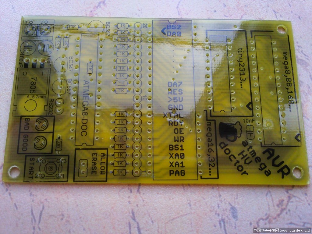
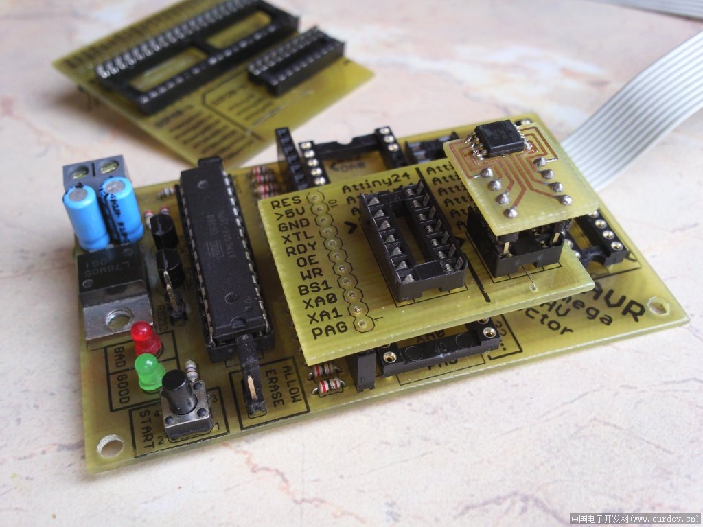
Just put your dead mega in socket, press the START button, and enjoy your good-as-new processor. There are three slots on board, for most common AVR’s, pins compatible with: Atmega8, Atmega16, Attiny2313. There is also an extra goldpin connector with all signals so you can attach adapters:
“#1 adapter” as HVPP extension, for 20pin Attiny26 compatible and 40pin Atmega8515 compatible processors.
“HVSP adapter” for 8pin and 14pin HVSP processors.
Or make your own adapters for other types of processors, in trough-hole or surface-mounted, you can use the breadboard for this – just connect signals to correct pins. How? Check your AVR datasheet, go to “memory programming” and then “parallel programming” – check the signal names, all signals are described under the DIP40 slot. In doctor memory there is a lot of free space so project may be developed all the time. One sided PCB with 55mm x 92mm dimensions. On top side you need to solder several jumpers, or, make this PCB as double sided – choose yourself. Resistors from R7 to R23 may be in 100ohm to 10K, but i suggest from 470ohm to 1K.
ATTENTION! While mounting the DIP40 slot, you must to remove it pins from 29 to 37. These pins must not have electrical contact with inserted uC pins, traces runs there only to make the board smaller (onesided). Take a look at pic on the left, these you must remove from slot.
Usage:
The ALLOW ERASE jumper allows doctor to erase whole flash and eeprom memory, if it is open, doctor will newer erase memory but may not cure device if lockbits are enabled, so you choose. After insert dead uC and press the START button, doctor will initiate the parallel or serial high-voltage programming mode. This is chosen automatically, device will recognize HVSP adapter and start to work in HVSP mode. After that, doctor wait for high state at RDY/BSY line. Then, read device signature and check if it supports it. Next, memory erase is performed if user allows that. Then lockbits are checked, and if they not blocking device, doctor sets all fusebits to fabric, having regard to whether there are extended fusebits or not. Some of older AVR have only one byte of fuses – LOW – and this is also included. After fusebits are verified, the proper leds is flashed.
Leds explanation:
green on – patient successfully cured, fusebits repaired. If lockbits are enabled, just verify fusebits with factory ones – and if they ok – light up green.
red on – signature problem, can’t read, no device in socket, or no such signature in database.
green flashing – signature ok, fusebits are wrong. Lockbits enabled, chip erase permission required (read below).
red flashing – signature ok, no lockbits, but for some reason can’t write new fusebits.
Terminal:
Note that terminal is not needed, device works without pc, and all we want to know we get from leds.
You can find extra RS232 output, and connecting this to the terminal, sends all information about fixing process – see exemplary printscreens in gallery. All the info is send “on fly” via uart. Use proper converter to connect this with pc. If you have COM port for RS232, use MAX232 based converter (eg this). If you are using laptop, use the USB converter (like this or this).
Terminal settings:
baudrate: 4800
parity: none
databits: 8
stopbits: 1
handshake: none
Other:
Use one of the following microcontrollers as the doctor-chip: Atmega88, Atmega88P, Atmega168, Atmega168P, Atmega328, Atmega328P – and their newer/low-voltage “A” or “L” versions.
Use stabilized 12V supply voltage. Higher voltage can damage fixed chip!
Code was written based on high-voltage parallel and serial programming section of datasheet of suitable AVRs.
If you are searching for attiny family AVR’s fusebits fix device, then check my previous project, the Attiny fusebit doctor. Unfortunately, some bugs show off and this project is no longer updated since the “Atmega fusebit doctor” supports all the Attiny family AVRs. But, source code is attached for this project, and with avr datasheet, it will be easy to understand this programming mechanism.
Fusebits:
Internal 1MHz clock, and enabled EESAVE bit – see README file.
If you use a brand new chips as doctor, you don’t need to change anything – 1MHz clock is already set as default. EESAVE bit is optional. It disallows to erase the eeprom when firmware is actualized, eeprom is used to store the fixed chips counter which is send trough uart.
FAQ – frequently asked Questions and Answers:
P: No sign of life, no leds are working.
O: Critical bugs on pcb, poorly programmed chip.
P: Red led is on.
O: Chip si not recognized. Make a voltage measurements. In idle, measure voltages on +12 RESET and +5 SUPPLY at female goldpin connector – you should get 0V or close to 0V on both. After the START button is pressed, you should get close to +12V and 5V for one second. If not, check transistors, if they are ok and if they are soldered ok.
Q: Red led is on.
A: Bugs on pcb, traces are packed densely and its very possible that you have invisible gap, shortcut, or dry joint. Check everything with multimeter, but PRECISELY.
Q: Red led is on.
A: Connect device to the terminal to get repair log. Press start to receive infos.
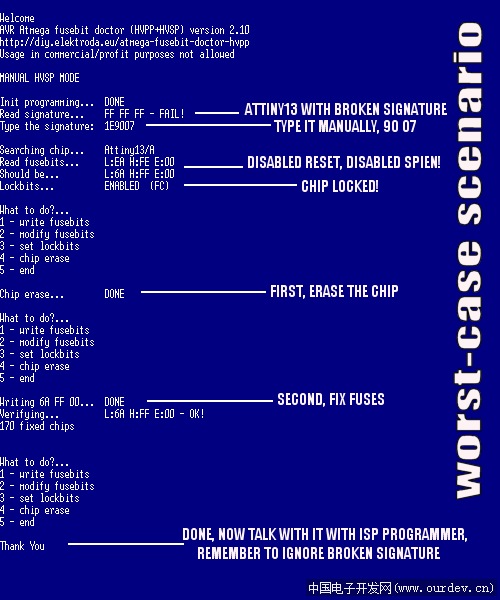
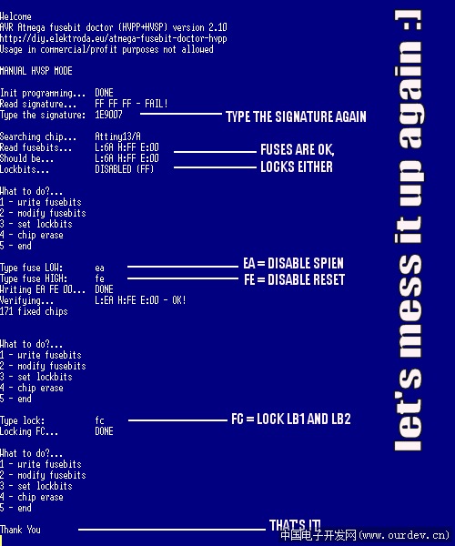
Q: Received “Init programming…” and nothing more – OR – received signature is “00 01 02″ or “FF FF FF”.
A: Chip is broken, or there still are bugs on pcb – look above.
Q: Received signature is “1E 90 00″, ” 1E 1E 1E”, or something familiar (meaningful data).
A: Chip is good, it initiates, look for shortcuts on DATA, BS, XA lines.
Q: Green led is on / “Verifying… – OK!” received, but chips don’t work with standard programmer.
A: You can be 100% sure that fuses are fixes, chip have hardware ISP damaged or it have some other damage.
Q: What are “Read Signature… FAIL!” and “Trying T2313 pinout… OK” doing in log?
A: Alle the 20pin chips need to be threated individually. First, device tries to read chip with standard schematic, and if it fails (“FAIL!”), then it tries to use schematic for 20pin T2313 compatible chips and then chip is read properly. This is normal behavior, this not a bug.
Q: What are “<[2J" trashes doing in log?
A: This is a terminal clear screen sequence, turn on the “VT-100″ emulation in terminal settings.
Q: I’m trying to type data into terminal but no chars appearing.
A:Make sure you set handshake to NONE in terminal settings.
Q: This still don’t help me, i tried everything but still have problem.
A: Ask in comments below :) Post firmware version and pcb version with which you try to work.
源文件(包括固件、主机板Eagle设计文档、转接板Eagle设计文档)可以在原网站上找到。这里把链接给大家:
http://diy.elektroda.eu/wp-content/uploads/2010/05/atmega-hvpp-fusebit-doctor_update11.rar
作为Doctor的那一枚ATMEGA8/88/168/328,需要烧写好程序设定好熔丝位之后再安装到板子上。原作者为每一个单片机给出了HEX和BIN烧写固件。其中MEGA88/168/328因为其内置Flash空间大,以ASCII码的形式存储了所有支持型号的名称——这只在连接电脑用串口通信的时候才会体现出来。而ATMEGA8的固件则没有,串口通信的时候显示signature正常,在支持表内,但不会显示具体型号,因为这样太占Flash空间。
其他的事宜,我想原网站讲的已经非常清楚了。不过他的FAQ中我想没有覆盖到一个常见的问题,而这个问题我遇到了,因此在下面列举出来:
Q: 我尝试修复任何AVR单片机,signature的读取都正常,芯片识别正常,然而就是总是写入新的熔丝位失败,怎么回事?
A: 根据ATMEL官方数据手册,并行高压编程下,读取的指令,DATA的高四位总是零,而写入的命令,DATA的高四位不全为零。因此请仔细检查你的DATA[7:4]的走线是否连通,串接电阻值是否正确。
这个网站我觉得很不错,尤其是最赞的就是他的网站上的《印制电路板详尽攻略 Printed circuit boards A to Z》,只可惜这篇文章连英文翻译都没有,只给你波兰文。感兴趣的童鞋可以去看一下。
http://diy.elektroda.eu/plytki-drukowane-od-a-do-z/?lang=en |
阿莫论坛20周年了!感谢大家的支持与爱护!!
知道什么是神吗?其实神本来也是人,只不过神做了人做不到的事情 所以才成了神。 (头文字D, 杜汶泽)
|


 发表于 2011-9-6 23:41:34
 楼主
楼主