|
|

楼主 |
发表于 2011-1-4 19:37:53
|
显示全部楼层
/****************************************************************
* Skyler Schneider ss868 *
* ECE 5760 Final Project *
* Sand Game *
****************************************************************/
module DE2_TOP (
// Clock Input
input CLOCK_27, // 27 MHz
input CLOCK_50, // 50 MHz
input EXT_CLOCK, // External Clock
// Push Button
input [3:0] KEY, // Pushbutton[3:0]
// DPDT Switch
input [17:0] SW, // Toggle Switch[17:0]
// 7-SEG Display
output [6:0] HEX0, // Seven Segment Digit 0
output [6:0] HEX1, // Seven Segment Digit 1
output [6:0] HEX2, // Seven Segment Digit 2
output [6:0] HEX3, // Seven Segment Digit 3
output [6:0] HEX4, // Seven Segment Digit 4
output [6:0] HEX5, // Seven Segment Digit 5
output [6:0] HEX6, // Seven Segment Digit 6
output [6:0] HEX7, // Seven Segment Digit 7
// LED
output [8:0] LEDG, // LED Green[8:0]
output [17:0] LEDR, // LED Red[17:0]
// UART
output UART_TXD, // UART Transmitter
input UART_RXD, // UART Receiver
// IRDA
output IRDA_TXD, // IRDA Transmitter
input IRDA_RXD, // IRDA Receiver
// SDRAM Interface
inout [15:0] DRAM_DQ, // SDRAM Data bus 16 Bits
output [11:0] DRAM_ADDR, // SDRAM Address bus 12 Bits
output DRAM_LDQM, // SDRAM Low-byte Data Mask
output DRAM_UDQM, // SDRAM High-byte Data Mask
output DRAM_WE_N, // SDRAM Write Enable
output DRAM_CAS_N, // SDRAM Column Address Strobe
output DRAM_RAS_N, // SDRAM Row Address Strobe
output DRAM_CS_N, // SDRAM Chip Select
output DRAM_BA_0, // SDRAM Bank Address 0
output DRAM_BA_1, // SDRAM Bank Address 0
output DRAM_CLK, // SDRAM Clock
output DRAM_CKE, // SDRAM Clock Enable
// Flash Interface
inout [7:0] FL_DQ, // FLASH Data bus 8 Bits
output [21:0] FL_ADDR, // FLASH Address bus 22 Bits
output FL_WE_N, // FLASH Write Enable
output FL_RST_N, // FLASH Reset
output FL_OE_N, // FLASH Output Enable
output FL_CE_N, // FLASH Chip Enable
// SRAM Interface
inout [15:0] SRAM_DQ, // SRAM Data bus 16 Bits
output [17:0] SRAM_ADDR, // SRAM Address bus 18 Bits
output SRAM_UB_N, // SRAM High-byte Data Mask
output SRAM_LB_N, // SRAM Low-byte Data Mask
output SRAM_WE_N, // SRAM Write Enable
output SRAM_CE_N, // SRAM Chip Enable
output SRAM_OE_N, // SRAM Output Enable
// ISP1362 Interface
inout [15:0] OTG_DATA, // ISP1362 Data bus 16 Bits
output [1:0] OTG_ADDR, // ISP1362 Address 2 Bits
output OTG_CS_N, // ISP1362 Chip Select
output OTG_RD_N, // ISP1362 Write
output OTG_WR_N, // ISP1362 Read
output OTG_RST_N, // ISP1362 Reset
output OTG_FSPEED, // USB Full Speed, 0 = Enable, Z = Disable
output OTG_LSPEED, // USB Low Speed, 0 = Enable, Z = Disable
input OTG_INT0, // ISP1362 Interrupt 0
input OTG_INT1, // ISP1362 Interrupt 1
input OTG_DREQ0, // ISP1362 DMA Request 0
input OTG_DREQ1, // ISP1362 DMA Request 1
output OTG_DACK0_N, // ISP1362 DMA Acknowledge 0
output OTG_DACK1_N, // ISP1362 DMA Acknowledge 1
// LCD Module 16X2
inout [7:0] LCD_DATA, // LCD Data bus 8 bits
output LCD_ON, // LCD Power ON/OFF
output LCD_BLON, // LCD Back Light ON/OFF
output LCD_RW, // LCD Read/Write Select, 0 = Write, 1 = Read
output LCD_EN, // LCD Enable
output LCD_RS, // LCD Command/Data Select, 0 = Command, 1 = Data
// SD Card Interface
inout SD_DAT, // SD Card Data
inout SD_DAT3, // SD Card Data 3
inout SD_CMD, // SD Card Command Signal
output SD_CLK, // SD Card Clock
// I2C
inout I2C_SDAT, // I2C Data
output I2C_SCLK, // I2C Clock
// PS2
input PS2_DAT, // PS2 Data
input PS2_CLK, // PS2 Clock
// USB JTAG link
input TDI, // CPLD -> FPGA (data in)
input TCK, // CPLD -> FPGA (clk)
input TCS, // CPLD -> FPGA (CS)
output TDO, // FPGA -> CPLD (data out)
// VGA
output VGA_CLK, // VGA Clock
output VGA_HS, // VGA H_SYNC
output VGA_VS, // VGA V_SYNC
output VGA_BLANK, // VGA BLANK
output VGA_SYNC, // VGA SYNC
output [9:0] VGA_R, // VGA Red[9:0]
output [9:0] VGA_G, // VGA Green[9:0]
output [9:0] VGA_B, // VGA Blue[9:0]
// Ethernet Interface
inout [15:0] ENET_DATA, // DM9000A DATA bus 16Bits
output ENET_CMD, // DM9000A Command/Data Select, 0 = Command, 1 = Data
output ENET_CS_N, // DM9000A Chip Select
output ENET_WR_N, // DM9000A Write
output ENET_RD_N, // DM9000A Read
output ENET_RST_N, // DM9000A Reset
input ENET_INT, // DM9000A Interrupt
output ENET_CLK, // DM9000A Clock 25 MHz
// Audio CODEC
inout AUD_ADCLRCK, // Audio CODEC ADC LR Clock
input AUD_ADCDAT, // Audio CODEC ADC Data
inout AUD_DACLRCK, // Audio CODEC DAC LR Clock
output AUD_DACDAT, // Audio CODEC DAC Data
inout AUD_BCLK, // Audio CODEC Bit-Stream Clock
output AUD_XCK, // Audio CODEC Chip Clock
// TV Decoder
input [7:0] TD_DATA, // TV Decoder Data bus 8 bits
input TD_HS, // TV Decoder H_SYNC
input TD_VS, // TV Decoder V_SYNC
output TD_RESET, // TV Decoder Reset
// GPIO
inout [35:0] GPIO_0, // GPIO Connection 0
inout [35:0] GPIO_1 // GPIO Connection 1
);
//Turn off all displays.
assign HEX0 = 7'h7F;
assign HEX1 = 7'h7F;
assign HEX2 = 7'h7F;
assign HEX3 = 7'h7F;
assign HEX4 = 7'h7F;
assign HEX5 = 7'h7F;
assign HEX6 = 7'h7F;
assign HEX7 = 7'h7F;
assign LEDR = 18'h0;
assign LEDG = 9'h0;
//Set all GPIO to tri-state.
assign GPIO_0 = 36'hzzzzzzzzz;
assign GPIO_1 = 36'hzzzzzzzzz;
//Disable audio codec.
assign AUD_DACDAT = 1'b0;
assign AUD_XCK = 1'b0;
//Disable DRAM.
assign DRAM_ADDR = 12'h0;
assign DRAM_BA_0 = 1'b0;
assign DRAM_BA_1 = 1'b0;
assign DRAM_CAS_N = 1'b1;
assign DRAM_CKE = 1'b0;
assign DRAM_CLK = 1'b0;
assign DRAM_CS_N = 1'b1;
assign DRAM_DQ = 16'hzzzz;
assign DRAM_LDQM = 1'b0;
assign DRAM_RAS_N = 1'b1;
assign DRAM_UDQM = 1'b0;
assign DRAM_WE_N = 1'b1;
//Disable Ethernet.
assign ENET_CLK = 1'b0;
assign ENET_CS_N = 1'b1;
assign ENET_CMD = 1'b0;
assign ENET_DATA = 16'hzzzz;
assign ENET_RD_N = 1'b1;
assign ENET_RST_N = 1'b1;
assign ENET_WR_N = 1'b1;
//Disable flash.
assign FL_ADDR = 22'h0;
assign FL_CE_N = 1'b1;
assign FL_DQ = 8'hzz;
assign FL_OE_N = 1'b1;
assign FL_RST_N = 1'b1;
assign FL_WE_N = 1'b1;
//Disable LCD.
assign LCD_BLON = 1'b0;
assign LCD_DATA = 8'hzz;
assign LCD_EN = 1'b0;
assign LCD_ON = 1'b0;
assign LCD_RS = 1'b0;
assign LCD_RW = 1'b0;
//Disable OTG.
assign OTG_ADDR = 2'h0;
assign OTG_CS_N = 1'b1;
assign OTG_DACK0_N = 1'b1;
assign OTG_DACK1_N = 1'b1;
assign OTG_FSPEED = 1'b1;
assign OTG_DATA = 16'hzzzz;
assign OTG_LSPEED = 1'b1;
assign OTG_RD_N = 1'b1;
assign OTG_RST_N = 1'b1;
assign OTG_WR_N = 1'b1;
//Disable SDRAM.
assign SD_DAT = 1'bz;
assign SD_CLK = 1'b0;
//Disable all other peripherals.
assign I2C_SCLK = 1'b0;
assign IRDA_TXD = 1'b0;
//assign TD_RESET = 1'b0;
assign TDO = 1'b0;
assign UART_TXD = 1'b0;
/**************************************************
* Clock and Reset Generation *
**************************************************/
wire SYSTEM_CLK;
VGA_PLL p1 (
.inclk0 (CLOCK_27),
.c0 (VGA_CLK),
.c1 (SYSTEM_CLK)
);
wire DLY_RST;
Reset_Delay r0 (
.iCLK (SYSTEM_CLK),
.oRESET (DLY_RST)
);
wire Reset;
assign Reset = ~DLY_RST;
/**************************************************
* Random Number Generator *
**************************************************/
wire [3:0] wRand4;
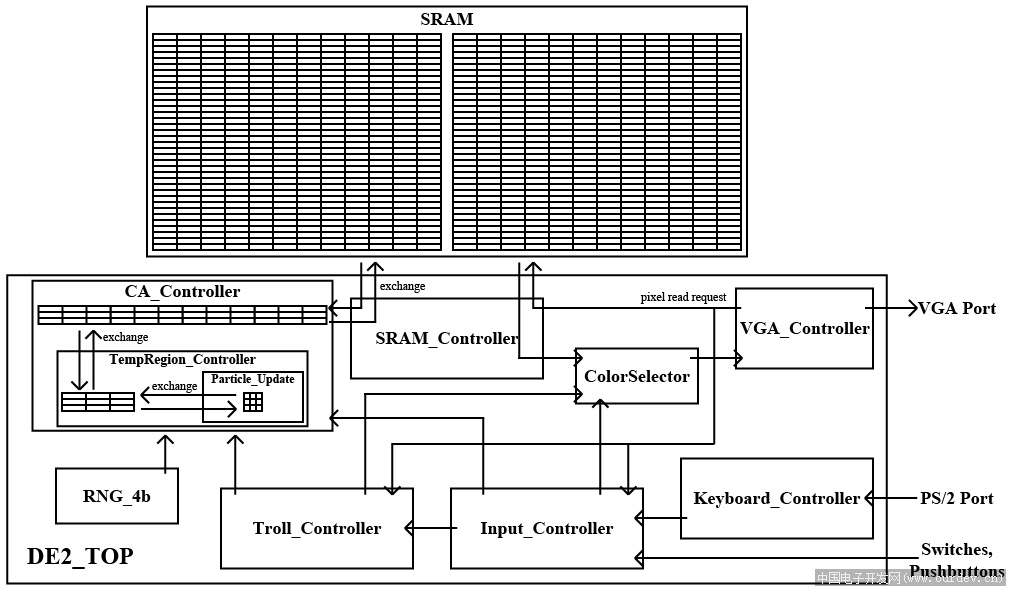
RNG_4b rng0 (
.iCLK (SYSTEM_CLK),
.iReset (Reset),
.oRandomNum (wRand4)
);
/**************************************************
* VGA Control Logic *
**************************************************/
assign TD_RESET = 1'b1; // Allow 27 MHz
wire [9:0] wVGA_R;
wire [9:0] wVGA_G;
wire [9:0] wVGA_B;
wire [18:0] wVGA_ADDR;
wire [9:0] wVGA_X;
wire [9:0] wVGA_Y;
wire wNewFrame;
wire [4:0] wSystemState;
VGA_Controller u1 (
// Control Signal
.iCLK (SYSTEM_CLK),
.iRESET (Reset),
// Host Side
.iRed (wVGA_R),
.iGreen (wVGA_G),
.iBlue (wVGA_B),
.oAddress (wVGA_ADDR),
.oCoord_X (wVGA_X),
.oCoord_Y (wVGA_Y),
.oSystemState (wSystemState),
.oNewFrame (wNewFrame),
// VGA Side
.oVGA_R (VGA_R),
.oVGA_G (VGA_G),
.oVGA_B (VGA_B),
.oVGA_H_SYNC (VGA_HS),
.oVGA_V_SYNC (VGA_VS),
.oVGA_SYNC (VGA_SYNC),
.oVGA_BLANK (VGA_BLANK)
);
wire [3:0] wSRAM_Color;
ColorSelector cs0 (
.iCLK (SYSTEM_CLK),
.iSystemState (wSystemState[2:0]),
.iVGA_X (wVGA_X),
.iVGA_Y (wVGA_Y),
.iSRAM_Color (wSRAM_Color),
.iCursor_X (wCursorX),
.iCursor_Y (wCursorY),
.iCursor_Size (wCursorSize),
.iTrollColor (wTrollColor),
.oVGA_R (wVGA_R),
.oVGA_G (wVGA_G),
.oVGA_B (wVGA_B)
);
/**************************************************
* SRAM Arbitration *
**************************************************/
SRAM_Controller sc0 (
.iCLK (SYSTEM_CLK),
.iRESET (Reset),
.iSystemState (wSystemState[2:0]),
.iNewFrame (wNewFrame),
.iVGA_ADDR (wVGA_ADDR),
.oVGA_Color (wSRAM_Color),
.iCA_ReadAddr (wCA_ReadAddr),
.oCA_ReadData (wCA_ReadData),
.iCA_WriteAddr (wCA_WriteAddr),
.iCA_WriteData (wCA_WriteData),
.iCA_WriteEn (wCA_WriteEn),
.SRAM_DQ (SRAM_DQ),
.oSRAM_ADDR (SRAM_ADDR),
.oSRAM_UB_N (SRAM_UB_N),
.oSRAM_LB_N (SRAM_LB_N),
.oSRAM_WE_N (SRAM_WE_N),
.oSRAM_CE_N (SRAM_CE_N),
.oSRAM_OE_N (SRAM_OE_N)
);
/**************************************************
* CA State Machine *
**************************************************/
wire [16:0] wCA_ReadAddr;
wire [15:0] wCA_ReadData;
wire [16:0] wCA_WriteAddr;
wire [15:0] wCA_WriteData;
wire wCA_WriteEn;
CA_Controller cc0 (
.iCLK (SYSTEM_CLK),
.iRESET (wFrameReset),
.iSTALL (wFrameHold),
.iSystemState (wSystemState[2:0]),
.iNewFrame (wNewFrame),
.iRand4 (wRand4),
.iTrollFlame (wTrollFlame),
.iCursorColor (wCursorColor),
.iCursorSize (wCursorSize),
.iCursorX (wCursorX),
.iCursorY (wCursorY),
.iCursorDraw (wCursorDraw),
.iFaucetSize_SAND (wFaucetSize_SAND),
.iFaucetSize_WATER (wFaucetSize_WATER),
.iFaucetSize_SALT (wFaucetSize_SALT),
.iFaucetSize_OIL (wFaucetSize_OIL),
.oReadAddr (wCA_ReadAddr),
.iReadData (wCA_ReadData),
.oWriteAddr (wCA_WriteAddr),
.oWriteData (wCA_WriteData),
.oWriteEn (wCA_WriteEn)
);
/**************************************************
* User Input *
**************************************************/
wire wKeyboardEventReady;
wire [7:0] wKeyboardEventType;
Keyboard_Controller kc0 (
.iPS2_CLK (PS2_CLK),
.iPS2_DAT (PS2_DAT),
.iCLK (SYSTEM_CLK),
.iRESET (Reset),
.oEventReady (wKeyboardEventReady),
.oEventType (wKeyboardEventType)
);
wire [3:0] wCursorColor;
wire [3:0] wCursorSize;
wire [9:0] wCursorX;
wire [9:0] wCursorY;
wire wCursorDraw;
wire wFrameReset;
wire wFrameHold;
wire wTrollBegin;
wire [2:0] wFaucetSize_SAND;
wire [2:0] wFaucetSize_WATER;
wire [2:0] wFaucetSize_SALT;
wire [2:0] wFaucetSize_OIL;
Input_Controller ic0 (
.iCLK (SYSTEM_CLK),
.iRESET (Reset),
.iSystemState (wSystemState[2:0]),
.iNewFrame (wNewFrame),
.iSW (SW),
.iKEY (KEY),
.iEventReady (wKeyboardEventReady),
.iEventType (wKeyboardEventType),
.oCursorColor (wCursorColor),
.oCursorSize (wCursorSize),
.oCursorX (wCursorX),
.oCursorY (wCursorY),
.oCursorDraw (wCursorDraw),
.oFaucetSize_SAND (wFaucetSize_SAND),
.oFaucetSize_WATER (wFaucetSize_WATER),
.oFaucetSize_SALT (wFaucetSize_SALT),
.oFaucetSize_OIL (wFaucetSize_OIL),
.oFrameReset (wFrameReset),
.oFrameHold (wFrameHold),
.oTrollBegin (wTrollBegin)
);
wire wTrollFlame;
wire [1:0] wTrollColor;
Troll_Controller tc0 (
.iCLK (SYSTEM_CLK),
.iRESET (wFrameReset),
.iSTALL (wFrameHold),
.iNewFrame (wNewFrame),
.iTrollBegin (wTrollBegin),
.iVGA_X (wVGA_X),
.iVGA_Y (wVGA_Y),
.oTrollFlame (wTrollFlame),
.oTrollColor (wTrollColor)
);
endmodule |
|


 发表于 2011-1-4 19:16:59