|
|
http://lekernel.net/scrapbook/old/ula.html
(原文件名:ula_top.jpg)
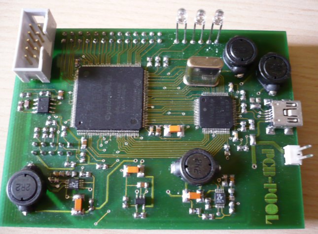
USB Logic Analyzer
The purpose of this board was to sample a reasonable number of logic channels (24) at a high rate, and stream the data to a computer through high-speed USB 2.0. But as this board is FPGA-based, it can be used for any application requiring a high transfer rate (hundreds of MBit/s) with a computer.
Technical description
The board uses a small Altera Cyclone II FPGA (EP2C5T144C7N) and a NET2272 USB controller from NetChip (this part is a bit hard to find, I got mine from Mouser Electronics). The FPGA was programmed with a mix of VHDL and schematic diagrams, and includes a minimal USB protocol handler entirely in hardware (no softcore processor was used).
The board can be self- or USB- powered. The 5V from USB is converted to 3.3V (used by the NET2272 and FPGA I/O) by a LTC3411 switching regulator and to 1.2V by another LTC3411 regulator (used by the FPGA core). The 3.3V supply is also converted to 2.5V by a linear regulator, and used to supply parts of the NET2272.
If you choose to replicate this device, please note there are a few stupid design errors in the files provided here (fortunately, they can be corrected with little board rework) :
The switching regulators need additional 100nF decoupling capacitors close to their input pins, or they can go unstable. IN EVERY CASE, DOUBLE-CHECK POWER SUPPLY VOLTAGES BEFORE SOLDERING THE FPGA AND THE NET2272 !
The wiring of the USB plug is incorrect, pin 5 is GND (not shield) and pin 4 can be left unconnected.
Bit 16 of the NET2272 bus is not connected to the FPGA (the NET2272 can operate in 8-bit mode anyway, but it's slower).
Also, Actel FPGAs seem better for this kind of project, but I went with the design tools I had available at that time.
The board is equipped with three connectors :
one 10-pin connector on top of the board is for JTAG configuration of the FPGA. Its pinout is the same as on Altera development boards, so you can directly use Altera Byteblaster cables for instance.
one 10-pin connector on the bottom is for connecting a serial FPGA configuration device
one 26-pin connector on the bottom is for connecting the probes (or whatever device you fancy ;-)
SMD soldering
It's a common myth that soldering small SMD parts such as TQFPs require lots of equipment. The board depicted above was entirely soldered by hand using an off-the-shelf soldering iron and a bit of inexpensive solder wick. A TQFP-144 can be soldered in about 10 minutes with very little equipment !
For SMD parts with a low pin count (ie. resistors, capacitors, small SOICs...) first make a solder ball on one of the PCB pads. Then heat it with the iron while plunging one pin of the part in the melted solder ball, with a pair of tweezers. Remove the soldering iron. You don't care if the solder is not good, its only purpose is to prevent the part from moving. Then, solder the other end of the component (be careful not to heat too much, not only you may damage the component but also you risk melting the first solder holding it), and rework the first solder.
Dont't mess around with SMD glue, it's a complete waste of time and money compared to this technique.
For SMD parts with a lot of small pins (ie. TQFPs, uMAXs, ...) you would go mad trying to solder each pin individually while avoiding short-circuits (and not heating the part too much !). First, prevent the part from moving using approximately the same technique as before : place the part very precisely using your hand or a pair of tweezers, then make a drop of solder on a couple of neighbouring pins (you don't care if you short them). Double check all pins are correctly placed on their corresponding PCB pads - it will be very difficult to correct an error afterwards. If they are not, melt the solder and carefully move the part. Once the part is correctly placed, make solder bumps on all pins, shorting them all together. Then, using solder wick, remove the excess solder which should go away easily, leaving just enough solder on each pin. Remove the solder residues this method leaves all around (nail polish dissolvent and a toothbrush work as good as flux cleaners, and is a lot cheaper. But get one without acetone, as it can damage some plastics). Visually inspect the connections (if they are short circuits, it is often easier to add a lot of solder over the shorted pins then to remove it using the wick).
I still need to find out about BGAs and QFNs (I've heard about messing with cooking ovens), fortunately this project uses none !
Downloads
Board schematics (PDF)
Board layout (PDF)
Altium Designer files (includes schematics, libraries, and routed PCB)
FPGA programming files (includes Quartus II project, schematics and VHDL code)
Quickly and badly written Linux driver (creates a device node from which you directly read 8-bit samples) |
阿莫论坛20周年了!感谢大家的支持与爱护!!
知道什么是神吗?其实神本来也是人,只不过神做了人做不到的事情 所以才成了神。 (头文字D, 杜汶泽)
|


 发表于 2010-7-28 21:21:24
 楼主
楼主