搜索
bottom↓
回复: 36

High Voltage Regulators

[复制链接]

出0入0汤圆

发表于 2009-8-28 23:17:52 | 显示全部楼层 |阅读模式
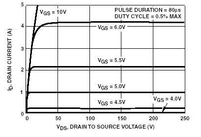
IC regulators like LM317 typically are good for up to 40v, not much more for the HV versions.

Tube amplifiers typically require much higher voltage at very low current levels. so how do you use a low voltage regulator in such a high voltage situation?

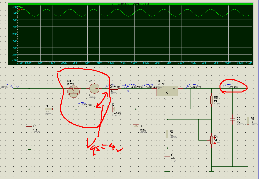
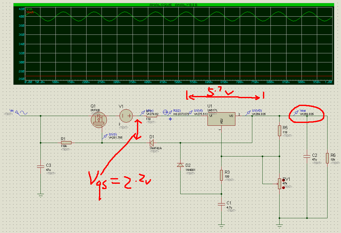
you use pre-regulation, like the Maida Regulator. In a pre-regulation, you use another high voltage device, either a BJT or a MOSFET, to drop most of the voltages and then use a low voltage regulator, like LM317, to regulate the rest. This has the advantage of being able to regulate very high voltages - depending on the discrete regulator, yet at very low cost / parts count, and ripple rejection.

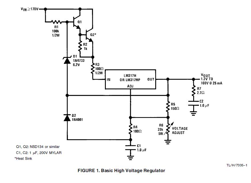
Here is a schematic for the Maida regulator.


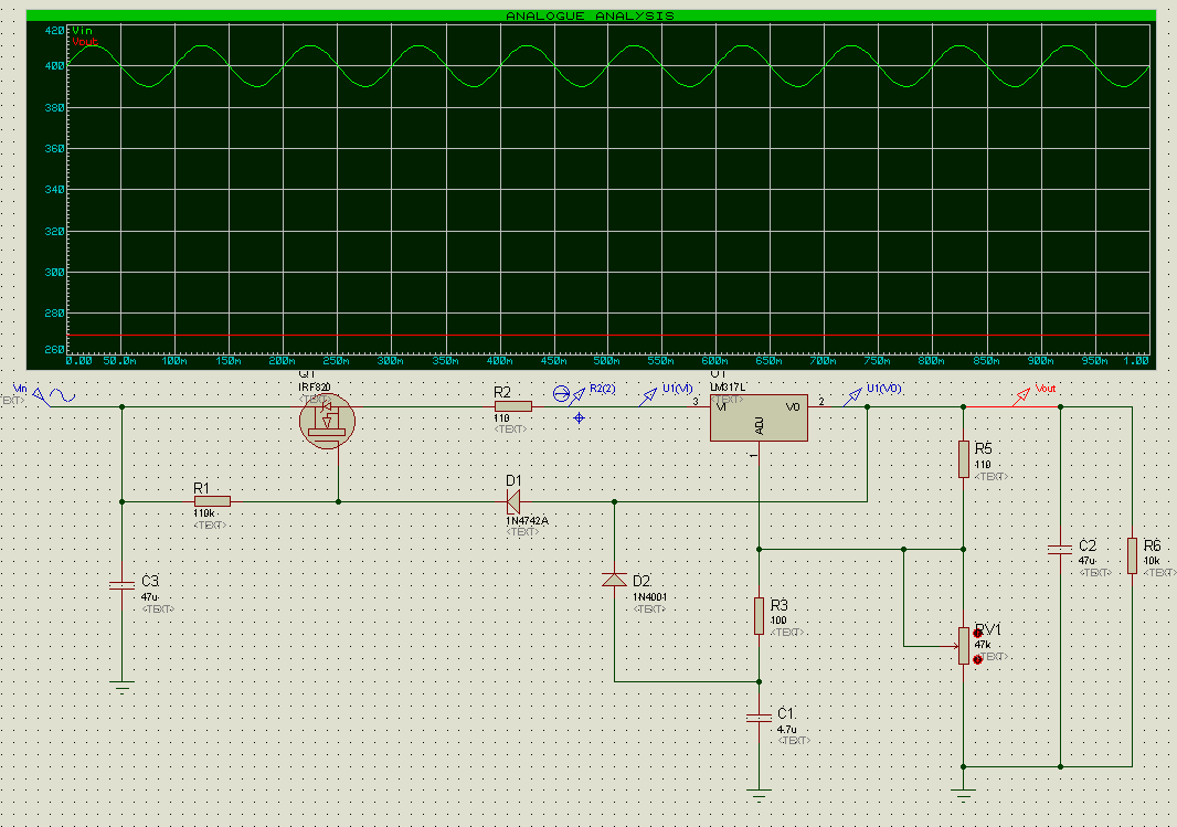
(原文件名:LM317 - Maida Regulator.PNG)

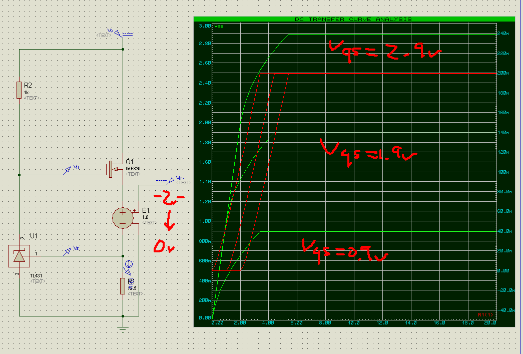
D1 controls the voltage drop over the IC regulator (=D1's Vz - Vgs - Iout*R2 = 6v). Output voltage is approximately 1.25v/R5*(R5+PV1).
Walter Jung also has a similar design.

阿莫论坛20周年了!感谢大家的支持与爱护!!

曾经有一段真挚的爱情摆在我的面前,我没有珍惜,现在想起来,还好我没有珍惜……

出0入0汤圆

发表于 2009-8-29 00:02:00 | 显示全部楼层
NS的原版电路Q1用的达林顿。
换成820,原有的过流保护精度低了。

原版的用过了,改了几处,与lz类似

317最小输出5mA,所以输出电压很高时电位器功率过大。100V5mA=500mW,所以后面用了10k

lz什么人?

出0入0汤圆

 楼主| 发表于 2009-8-29 05:11:11 | 显示全部楼层
yes, mosfet's relatively lower gm will reduce the open loop gain. But the gain is dominated by the lm317, so the loss of some gains on the regulator shouldn't be that big of a deal.

you can solve the pot dissipation issue by replacing it with a pot-controlled "variable" load, or a fixed voltage zener if you don't need the adjustability - ie a purpose-built power supply.

出0入0汤圆

发表于 2009-8-29 09:52:37 | 显示全部楼层
说差了
820的栅电压很难讲多大,没有BE结压降准,因此落在R2上的电压不准确,可能提前过流保护,也可能电流过了不保护

不过我一直在想换成MOS管,少一种库存。

出0入0汤圆

 楼主| 发表于 2009-8-29 18:42:50 | 显示全部楼层
"820的栅电压很难讲多大,没有BE结压降准,因此落在R2上的电压不准确,可能提前过流保护,也可能电流过了不保护 "

you don't need to know the Vgs: it only impacts the voltage drop on the lm317 and has no impact on the output voltage stability.

出0入0汤圆

发表于 2009-8-29 19:46:04 | 显示全部楼层
如果R2里流的电流比较大呢?
如果需要200mA而实际用到150mA,就很难说317的压降了,也很难保证输出正确。

当然这么用的机会不大,我一般都打一倍余量。

出0入0汤圆

 楼主| 发表于 2009-8-29 19:55:48 | 显示全部楼层
this power supply isn't for high current applications. it would be hard to hold the output voltage steady above 100ma: the power dissipation over the mosfet / bjt regulator would be too large.

if you do want to output more current, you can "reduce" the size of R2 and use a high voltage D1. the only purpose of R2 is to provide some negative feedback in case Vgs / Vbe goes down as the transistors heat-up. aka it is for thermal stability more than anything else.

出0入0汤圆

发表于 2009-8-29 21:02:47 | 显示全部楼层
确实,ls的Vin太高了。
我用到过200mA,总压降20V左右,过流保护300mA。加上散热器问题不大,4W而已。
Vgs和VD1是固定值,R2和317上的压降也是固定值,而且317的压降对电流不敏感,因此R2有过流保护的作用,当然,是靠负反馈。
如果无需过流保护,R2也可不用。

不用R2时开环增益比较高,可能反馈控制的状态稍差。

不容易,遇到行家。

Where do you come from?

出0入0汤圆

发表于 2009-8-29 21:27:43 | 显示全部楼层
shichen717,大多数MOSFET的转移特征曲线在200mA附近还是比较陡的,也就是说在这个电流下,Vgs基本上是一固定值,因而对限流精度影响不会很大。

出0入0汤圆

发表于 2009-8-29 21:38:57 | 显示全部楼层
不同的MOSFET的VGS离散性较大,同一批同一型号的VGS也有较大离散性,3V到4V不等。
同时,200mA附近的转移特性曲线与VDS有关,不同的VDS,IDS曲线形态也不同,对应200mA的VGS也不同。
如果总压降由20V提高到50V,有可能R2要重新设定,而由于VGS的离散性和对VDS的不确定性,R2的值只能靠每次实测,而非像Darlington的VBE一样只有100mV的差异。
况且,电源的输出电流由5mA至200mA不等,无法有相对稳定的VGS。

如图,820的IDS vs. VDS,用在VGS<4V的区域,此时gm变化较大。


(原文件名:未命名.JPG)


lz的电路没问题,只是改得出了一点儿小瑕疵,深入讨论一下,其优点在于R1更好选择。

出0入0汤圆

发表于 2009-8-29 22:21:04 | 显示全部楼层
【9楼】 shichen717,上面的图表并不能直观地看出VDS对VGS的影响,下面是一个仿真测试图,让820工作在恒流200mA状态,改变VD从5V到100V,测量VGS几乎为一直线,保持在4.5V左右。所以VDS对VGS影响很小(ID恒定时),至于同一型号不同批次的VGS差异,我印象中也就0.3V左右的上落,反而温度对VGS可能有些影响。

(原文件名:未命名.PNG)

出0入0汤圆

发表于 2009-8-29 22:48:50 | 显示全部楼层
首先,模型不能模拟器件离散度,对于指定的一支MOSFET,ls的理论成立,对于大量生产的产品,对离散性的考虑更重要。
其次,对于相同电流,Vgs的变化量可达300mV,darlington VBE的变化量小于100mV,这是双极器件相对单极器件的优势。
对于25欧姆的R2,100mV意味限流误差为4mA,300mV意味限流误差为12mA,同时考虑离散性,Vgs造成的限流误差可达到30mA以上,对于200mA的电源而言误差过大。
在此,既然过流保护,电流将大于200mA,设过流保护300mA,则200-300mA之间引起Vgs的变化将引起提早保护。
lz的电路不会只用在一种场合,假设限流分别为5mA、10mA、50mA、100mA、200mA、300mA的6种应用场合,用820很难预计R2的取值,而用darlington则可轻易做到相当准确的过流保护,这也是讨论的中心问题。

题外话:
ls的电路可能实际使用时会振荡,820的输入电容几百pF,不加频率补偿的情况下即使使用纯电阻性负载也可能不稳定,如果负载是电感,起振的可能性更大些。电容性负载应该比较稳定。
仿真的结果可能有偏差。之所以不振是因为所有电源都是理想的,没有纹波,而电源端可视为另一输入极,实际电源的纹波将成为引发起振的原因。
最简单应在栅极串联小电阻,此外采样可能不能直接进431。

出0入0汤圆

发表于 2009-8-29 23:44:12 | 显示全部楼层
10楼的仿真只是检验VDS对VGS影响,并没有考虑过多的细节,由结果看来,VDS的大幅变动对VGS影响很小,而影响VGS的主要因素看来是不同个体之间参数参数差异。要减少这种影响,可以提高稳压管的电压,不过这样将带来其它一些弊端。

出0入0汤圆

 楼主| 发表于 2009-8-29 23:55:41 | 显示全部楼层
"不用R2时开环增益比较高,可能反馈控制的状态稍差。 "

if you don't use R2, the circuit isn't stable thermally with vertical mosfet and you will have to use lateral mosfet. the only purpose of R2 is to improve the circuit's thermal stability. As a matter of fact, the circuit will achieve better regulation if you could get rid of r2.

"首先,模型不能模拟器件离散度,对于指定的一支MOSFET,ls的理论成立,对于大量生产的产品,对离散性的考虑更重要。 "

you can simulate cowboy's circuit with different mosfets, logic vs. conventional for example, and you will get the same results. that's the beauty of negative feedback.

"而用darlington则可轻易做到相当准确的过流保护,这也是讨论的中心问题。 "

R2 performs the same function if the regulator is a darlington. the "benefits" introduced by a bjt is the beta droop at higher temperature, which divers current away from the zener and partially compensates Vbe drop in the process.

because of high dissipation, this circuit can NOT be used when the load current is high, unless you purpose-build it.

出0入0汤圆

发表于 2009-8-30 00:23:10 | 显示全部楼层
lz电路可成功应用的前提是不热,无论R2如何,VdsIds都将产生热量。

散热才可解决温度问题,依靠R2进行热反馈的电路输出电流过小。

模拟的结果通常较好,因为无需考虑散热。如果VDS=100V,IDS=200mA,功率20W,温度造成的gm变化很明显,VGS自然不稳定。
实际应用中不可能不考虑温度造成的影响。

VBE在通常电路工作温度内均比较稳定,只是增益会有变化,然而预稳压无需过高的增益,没有必要保证R2和317的总压降十分稳定。使用Darlington可适当提高增益。事实上增益由200降至20误差不过由0.5%增大到5%,没有Vgs的影响大。
实际使用中KSP42+2SC3150足矣,200mA下的增益不低于100。

200mA我大量用过,控制好Vdrop,做好散热就没有问题,商用产品。只要解决散热,R2的热反馈作用可以基本不考虑。

这是NS的原版:


(原文件名:无标题.jpg)

出0入0汤圆

 楼主| 发表于 2009-8-30 00:50:57 | 显示全部楼层
"模拟的结果通常较好,因为无需考虑散热。如果VDS=100V,IDS=200mA,功率20W,温度造成的gm变化很明显,VGS自然不稳定。
实际应用中不可能不考虑温度造成的影响。 "

Vgs changes, due to thermal stress or otherwise, don't really matter, as long as the voltage across the LM317 doesn't get too low.

And Vgs changes will be offset by voltage changes on LM317 and LM317 has a good tolerance for fluctuations in input voltage - that's why it is a voltage regulator.

出0入0汤圆

 楼主| 发表于 2009-8-30 00:58:08 | 显示全部楼层
here is an example.

the circuit below is identical to what I posted earlier, with one exception: I added V1 to the mosfet's source to simulate Vgs declines when the mosfet heats up. so Q1+V1 equates to a "real" mosfet and by changing V1 we get to simulate the mosfet's temperature changes. a positive V1 will mean lower Vgs, thus a mosfet at higher temperature.


(原文件名:Maida Regulator 1.PNG)

the first graph shows V1=0, and Vgs = 281.7v - 277.5v=4.2v. Output Vout=269.7v.

出0入0汤圆

 楼主| 发表于 2009-8-30 01:06:31 | 显示全部楼层
Vishay's datasheet for IRF820 shows that Vgs goes down by about 1v with Id=300ma and Vds=50v, when case tempearture goes from 25c to 125c. Vgs decline is more at lower Id levels.

so to be conservative, I assume Vgs will go down by 2v (V1=2v). here is the simulation. everything else remain unchanged.


(原文件名:Maida Regulator 2.PNG)


as you can see, Vgs for the heated mosfet (inclusive of V1) is 281.8v-279.6v=2.2v. yet, output Vout stays at 269.8v, vs. 269.7v before. a 0.1v or 0.04% change.

出0入0汤圆

发表于 2009-8-30 01:11:34 | 显示全部楼层
有点乱
Vout从来也没出过问题。
问题在于Ilimit。
Vgs影响了Ilimit的准确度。

多数情况下,这个电路由于热量的问题不能承受过高电流,而实际可用的电流又比较接近Ilimit,例如200mA时Ilimit=300mA,事实上250mA也在可用范围内,但Ilimit不能再高了。改820后Ilimit的误差太大,从而限制了可用电流范围。

这只是一点瑕疵,如果Ilimit=300mA,而实际使用10mA就没问题。
高电压的功率电源本来就对参数要求比较苛刻,无需再加入一些可能出问题的部分造成烦恼。

我一度想过这么改,但考虑到此不确定因素,不得不维持原设计。

出0入0汤圆

 楼主| 发表于 2009-8-30 01:12:33 | 显示全部楼层
why?

in the first simulation, the voltage across the LM317 is 273.4v - 269.7v=3.7v.

in the 2nd simulation, the voltage across the LM317 is 275.5v - 269.8v=5.7v. the increase of 2v is exactly the opposite of that 2v decline in Vgs caused by the mosfet's tempco.

the 3.7v voltage differential is chosen is minimize power dissipation on the LM317, at the expensive of its ripple rejection - I am using LM317L here (a to92 device). if you use a to220 version of the LM317, you can afford to run the regulator a little bit hotter, by using a higher voltage D1: the voltage drop over the LM317 is approximately Vz (voltage drop over the zener) - Vgs (or Vbe if you used a bjt) - (Iout+1.25/R5)*R1.

出0入0汤圆

 楼主| 发表于 2009-8-30 01:21:30 | 显示全部楼层
"问题在于Ilimit。
Vgs影响了Ilimit的准确度。 "

this design has no current limit: if you were to short the output, the output current will be roughly (Vz - Vgs - Vdo)/R2 - 1.25 / R5). and in any way, it will kill your regulator because the thermal feedback is positive here.

that's true regardless of the type of devices used. with the bjt's 2ndary breakdown and smaller SOA, it will blew sooner and faster than a mosfet.

出0入0汤圆

发表于 2009-8-30 01:36:19 | 显示全部楼层
抱歉没看清317L,字有点小。

Ilimit是保护调整管和317两者的。317T可耐受1.5A电流,但不能超过TO220最大管耗限制。
同样道理,调整管+317的最大管耗限制了两者共同的输出电流。
调整管和317都可以耐受1A以上的电流,但组合在一起时,调整管承受的电压更高,因此耐受的电流Ilimit更小。
Ilimit在输出端短路时主要保护调整管。
正常工作下,Vdrop=30V,250mA只消耗8W功率,上10W散热器足矣。
试想100V输入时,300mA短路电流将产生30W功率,10W散热器时,调整管可以承受几分钟。
Ilimit再大就不好处理了,例如500mA,实际使用中不会真的给一个10W电源上50W散热器,而50W功率对于10W散热器太高了,几秒调整管就可能热击穿,超出人的反应能力,起不到保护作用。

因此Ilimit的限制在于短路保护,面对的是Vin,因而很苛刻,而使用电流的限制在于Vdrop,两个电流可能很接近。

this design has no current limit:
======================================
1N4742有12V,一旦短路,去除Vgs=4V,R2和317共承受8V。R2电流限制于80mA,保护了317L。调整管可能安全,也可能不安全,因此R2稍适偏小。

出0入0汤圆

 楼主| 发表于 2009-8-30 01:39:12 | 显示全部楼层
to add to cowboy's sim, here is my version that tries to introduce the mosfet's tempco into the analysis. I put in a voltage controlled voltage source to simulate the decrease in Vgs as the mosfet heats up. Again, I put the changes in Vgs to -2v, as you can see in the green traces.


(原文件名:tl431 Id vs Vgs.PNG)

the red traces show the current going through the resistor.

As you can see, once the rail voltage is enough to conduct the tl431 and get the mosfet to open, the current going through R1 does not change with Vgs variations at all. ie. the mosfet's tempco, thus Vgs variations, are irrelevant for this analysis.

出0入0汤圆

 楼主| 发表于 2009-8-30 01:46:08 | 显示全部楼层
"因此Ilimit的限制在于短路保护,面对的是Vin,因而很苛刻,而使用电流的限制在于Vdrop,两个电流可能很接近。"

current limit by R2 is minimal, and for practical purposes you should consider this topology to have no over current protection. That's true because of the topology, not because of the type of devices used.

if you short the output, the regulator will blow in a split of second, even if you have a large heatsink mounted.

you can improve its current stability:

1) by using negative tempco regulators. like lateral mosfets.
2) by using a small Vz zener. But that will negative impact your input voltage range and ripple rejection.
3) by using a large R2. you will thus reduce the open loop gain and hurt your ripple rejection.

...

end of the day, over current protection for high voltage power supplies is very difficult and you will have to rely on other means to achieve it. the over current protection in this particular circuit is minimal, at best.

出0入0汤圆

发表于 2009-8-30 01:59:24 | 显示全部楼层
if you short the output, the regulator will blow in a split of second, even if you have a large heatsink mounted
--------------------------------------------------------
曾经试过130V Vin,Ilimit=150mA,短路5分钟,一切无恙。

出0入0汤圆

 楼主| 发表于 2009-8-30 02:03:11 | 显示全部楼层
"1N4742有12V,一旦短路,去除Vgs=4V,R2和317共承受8V。R2电流限制于80mA,保护了317L。"

with the output shorted, the regulator IRF820 has a Vds=Vc - V(R2) - Vdo. Since Vc is far greater than others, Vds ~= Vc = 400v.

so its power dissipation is 400v*80ma = 32w. that will heat up the mosfet and drive down its Vgs, which in turn drives up the current going through the mosfet, which in turns drives down Vgs -> your mosfet will be gone in no time. and no amount of heatsink will save you.

出0入0汤圆

 楼主| 发表于 2009-8-30 02:08:29 | 显示全部楼层
"曾经试过130V Vin,Ilimit=150mA,短路5分钟,一切无恙。 "

you can do it for low voltage / low current applications if you design for it. if you are talking about 300ma application (with 2x of the heatroom) and taking 400v input for potentially 400v*2*300ma=240w dissipation on the regulator, you will have a lot of difficulties finding the right devices as regulators and drive those devices.

this topology is primarily a high voltage small current regulator.

you are far better off with other topologies for high voltage high current applications.

出0入0汤圆

发表于 2009-8-30 10:04:50 | 显示全部楼层
that will heat up the mosfet and drive down its Vgs, which in turn drives up the current going through the mosfet, which in turns drives down Vgs
=============================================================
??这个好像有点儿不对劲儿

出0入0汤圆

发表于 2011-1-10 05:21:02 | 显示全部楼层
mk

出0入0汤圆

发表于 2011-1-10 08:34:18 | 显示全部楼层
记号一下,阿莫什么时候加上收藏就好了

出0入0汤圆

发表于 2011-1-10 11:19:40 | 显示全部楼层
好帖!记号~~

同意楼上建议。

出0入0汤圆

发表于 2011-1-10 11:51:19 | 显示全部楼层
MARK 调压器
MARK Regulator
MARK 电源

出0入0汤圆

发表于 2011-8-5 10:26:09 | 显示全部楼层
mark

出0入0汤圆

发表于 2011-11-16 11:55:11 | 显示全部楼层
全部都是是英文!!!!!!

出0入0汤圆

发表于 2012-2-21 15:31:41 | 显示全部楼层
mark

出0入0汤圆

发表于 2012-2-22 13:51:02 | 显示全部楼层
再顶,慢慢看

出0入0汤圆

发表于 2012-3-5 16:20:17 | 显示全部楼层
好贴,怎么感觉两位高手一个在说原设计一个在说本设计;呵呵

有几个问题:

1,6楼millwood0大师说的R2 is to provide some negative feedback in case vgs goes down as the transistor heat

请教:您此时说的调整管过热,是因为regulator的散热不好还是因为电流的上升导致的呢??

两种不同的情况反馈的情况也应该不一样;

对于散热不好的反馈:T升高---Vgs下降---因Vg不变----Vs上升-----Vds减小----因I不变---Vds*I 减小---P功率减小  ;        

此时R也没参与其中啊??也就是说为何R2控制电路温度的稳定性;

为何去掉R2会有更好的纹波抑制???为何增大R2,纹波抑制能力变弱呢?


2,7楼shichen大侠说的不用R2时开环增益比较高,平时都说的是运放方面,一说到这就不会了;此时的开环增益是怎么算的呢??把反

馈器件D1去掉,之后再怎么求开环增益呢??


3,11楼shichen大侠说的题外话,为何不同负载时,振荡情况不一样呢??


4,vertical mosfet 和lateral mosfet应该如何理解呢??横向竖向???
回帖提示: 反政府言论将被立即封锁ID 在按“提交”前,请自问一下:我这样表达会给举报吗,会给自己惹麻烦吗? 另外:尽量不要使用Mark、顶等没有意义的回复。不得大量使用大字体和彩色字。【本论坛不允许直接上传手机拍摄图片,浪费大家下载带宽和论坛服务器空间,请压缩后(图片小于1兆)才上传。压缩方法可以在微信里面发给自己(不要勾选“原图),然后下载,就能得到压缩后的图片。注意:要连续压缩2次才能满足要求!!】。另外,手机版只能上传图片,要上传附件需要切换到电脑版(不需要使用电脑,手机上切换到电脑版就行,页面底部)。
您需要登录后才可以回帖 登录 | 注册

本版积分规则

手机版|Archiver|amobbs.com 阿莫电子技术论坛 ( 粤ICP备2022115958号, 版权所有:东莞阿莫电子贸易商行 创办于2004年 (公安交互式论坛备案:44190002001997 ) )

GMT+8, 2024-8-26 11:27

© Since 2004 www.amobbs.com, 原www.ourdev.cn, 原www.ouravr.com

快速回复 返回顶部 返回列表